Frequently Asked Questions About Sputtering
Estimated reading time: 7 minutes
Sputtering, in material science, is a phenomenon in which a material is bombarded with energetic particles which in turn ejects particles of the material onto a substrate, which forms a microscopic thin layer of the material onto the substrate. It is one of the common physical vapor deposition techniques widely used in the thin film coating industry.
If you want to see a video of sputtering in action, click this link to be directed to our YouTube video of high-temperature sputtering. The purple glow you notice is the target material as a plasma that is being deposited onto Aluminum (Al) foil.
Watch Sputtering in Action
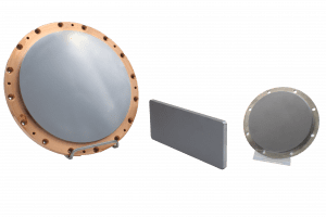
The word ‘target’ refers to the material which the plasma is ‘targeting’ or sending energetic particles towards. A sputtering target is a dense material composed of the compounds or pure elements manufacturers need in their thin-film coatings.
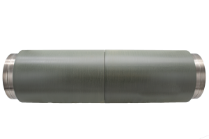
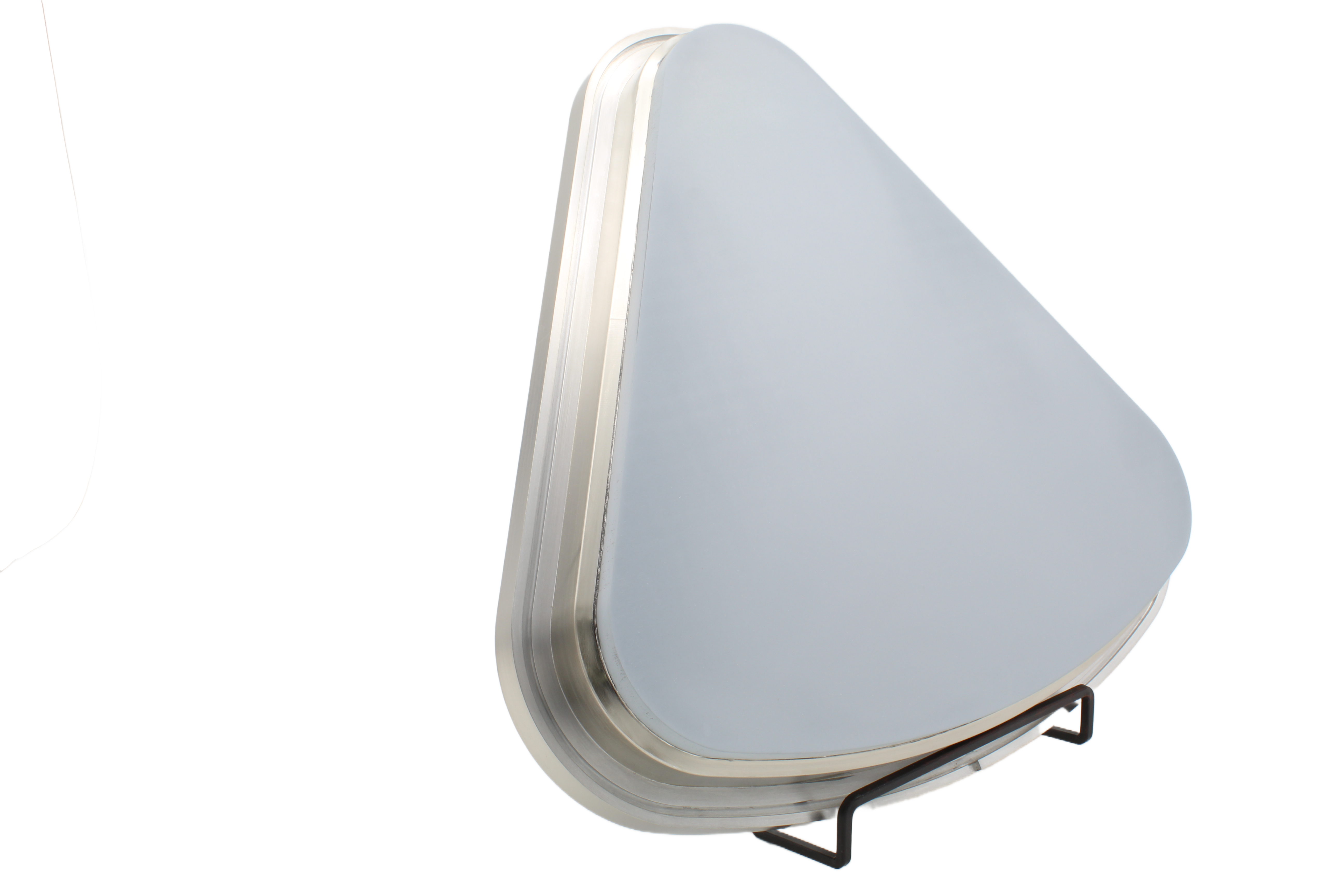
Sputtering targets can vary in shape from circular to triangular or rectangular and even be cylinders in roll-to-roll applications. Some are composed of single pieces, while others are large multi-tile configurations.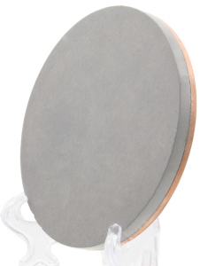

Sputtering is a ubiquitous thin-film coating technique used in many facets of manufacturing. Lenses in sunglasses are coated with a material that will block certain bandwidths of light. Cellular phones contain a sputtered layer of Transparent Conductive Oxide (TCO) which creates touchscreen capabilities. Thin-film solar panels utilize thin and flexible layers of sputtered material to create stacks that convert light into electricity. Computer chips are created using selective sputtering and photomasking. These are just some of the ways sputtering targets are used in commercial products.
We use Indium (In) to bond sputtering targets to backing plates. This layer between the target and the backing plate starts as a liquid, filling up any void or irregularities. When it cools it creates a solid yet malleable bond between the backing plate and target. The thermal expansion of the target and the backing plate often differ tremendously. We use Indium to reduce the risk of the whole assembly warping while it is in use. Additionally, Indium adheres better than almost any other solder-like material.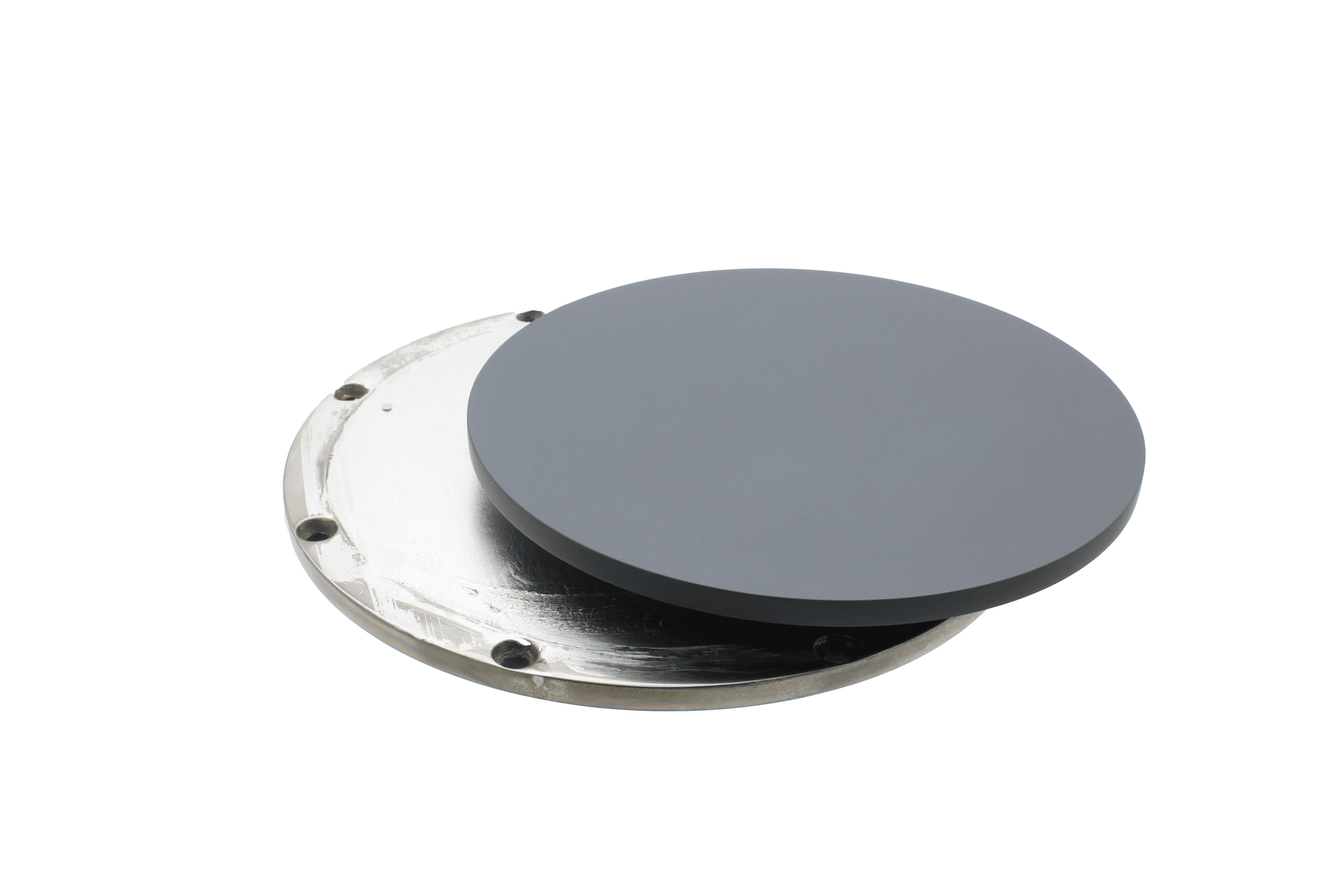
Sputtering is a form of thin-film deposition. Thin-film deposition, accompanied by photo masking, is used to create micro-circuits and dielectric gates which are integral to microchip production.
The video below, produced by Infineon Technologies AG, is fantastic in explaining the journey “from sand to semiconductor”
http://https://www.youtube.com/watch?v=bor0qLifjz4
Since SCI Engineered Materials can create multi-tile assemblies, there is no limit to the size of an assembly we can produce. Our largest in-house dies are 8.7″ x 8.7″, 14.95″ x 6.56″, and 12.250″ dia which represent approximately the largest single tiles we can produce.
The type of sputtering used depends heavily on whether the target material is conductive or not. In DC sputtering, the target material must be conductive, though the process is done fairly quickly. RF sputtering utilizes the electromagnetic field created by radio waves to bombard the substrate with the target material. RF sputtering doesn’t need the target material to be conductive, however, this method is extremely slow. Typically we see prototype and proof-of-concept designs utilize RF sputtering, while matured concepts & applications utilize DC sputtering
Sputtering is a type of thin-film deposition.
Sputtering can naturally occur, and there is some evidence that ancient civilizations may have known about the concepts of deposition and thin films. The patent for the modern process was filed by Frans Michel Penning on November 7th, 1936, patent number US2146025A under the name “Coating by cathode disintegration”.
Sintering is the process of compacting a material through high temperatures and pressure without melting/liquifying the material. This is one step in the process of creating ceramic sputtering targets.
Sputtering targets are consumable materials that manufacturers and researchers use to create thin-film coatings. Sputtering targets, or target assemblies, are latched or bolted, or sometimes magnetically held in the coating chamber.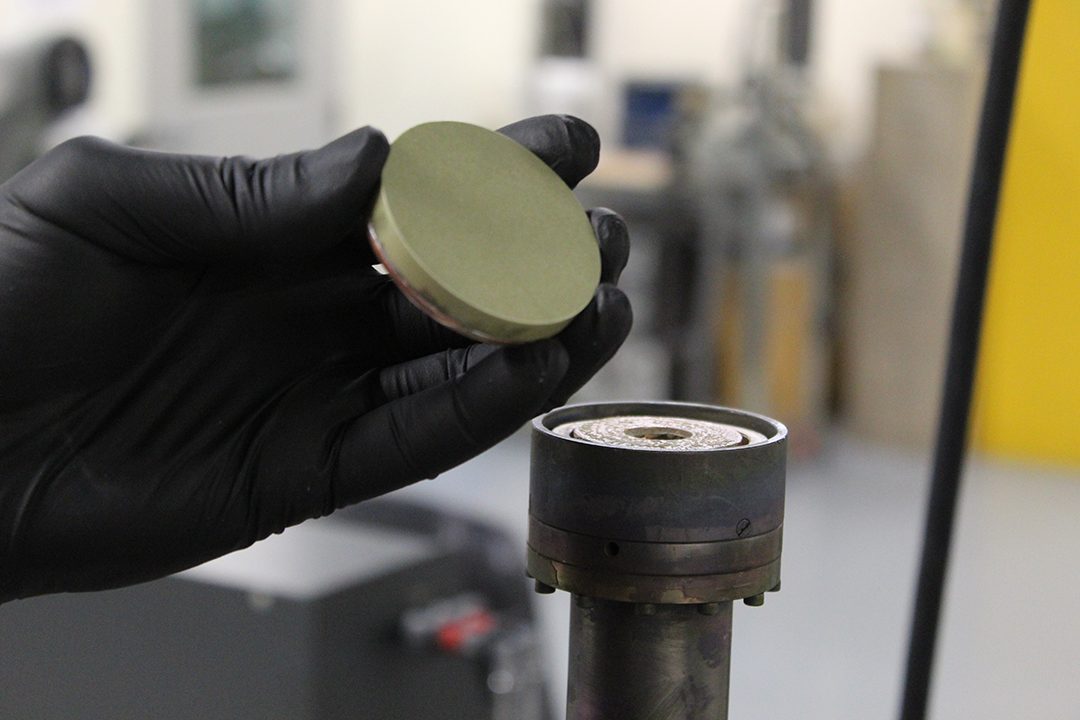
Quality control & assurance is one of the pillars of our company’s success. In order to control the quality of our products, we have strict vetting processes for raw material suppliers and very specific raw material specifications that have been tried and tested in our processes. Furthermore, when issues do arise from raw material batches, SCI Engineered Materials is best suited to address those issues directly with the raw material supplier since we can provide in-depth data on batch issues.
Since we cannot properly verify the source or specifications of customer-supplied powder, and since the direct relationship between SCI Engineered Materials and its raw material suppliers is more efficient and less susceptible to miscommunication we reserve the right to refuse customer-supplied powder pressing requests.
However, if you need diffusion bonding, or can properly verify the source material we may be able to assist! Send us a quote request to see how we can help.
To get a good idea of where these materials begin their journey, take a look at this interactive map from the United States Geological Survey of where deposits are around the world:
https://mrdata.usgs.gov/major-deposits/map-us.html
Some materials like Zinc Oxide (ZnO), are rare in nature, but extremely easy to produce in commercial laboratory settings. However, the beginning raw material, in this case, Zinc, would still need to be sourced from the mine/refinery.
Additionally, SCI Engineered Materials strictly adheres to the Conflict Minerals provisions of the Dodd-Frank Wall Street Reform and Consumer Protection Act, HR 4173, Section 1502 (“Conflict Minerals Act”) This means that we will work with our suppliers and take appropriate actions to ensure that our products do not contain conflict minerals. These actions will include conducting reasonable country of origin inquiries and, as necessary, obtaining reliable certificates of origin for all materials that might possibly originate in the Democratic Republic of the Congo (DRC) areas or an adjoining country.
Due to recent events in the year 2022, we find it important to ensure our customers that none of our materials are sourced from the Russian Federation.
If you’re a raw material supplier who would like to start a relationship with SCI Engineered Materials, reach out to us via email at sales@sciengineeredmaterials.com and let us know what kinds of materials you provide.
Since we are an ISO 9001:2015 certified company, our production staff is well-versed and trained in documenting processes and following meticulously detailed instructions. When provided, we can even video-document procedures for enhanced customer assurance. Since the machinery and technology we use can be dangerous when operated by untrained hands, we can not allow customers to operate machinery.
If you’d like to request one of our toll services visit our Request a Quote page and tell us more about your needs.